School of Electrical Engineering, Electronics and Automation

Wednesday, 26 August 2020

AC Motor control - Frequency converter


Motor control - Frequency converter - TESLA Institute 


A complete installation with a frequency converter controlled motor consists of a series of different components which should all be selected carefully for a given application.


The components in an installation are selected according to the actual application, starting with selecting the right pump for the application. A suitable motor for the actual pump is chosen. The output filter of the frequency converter has to be able to handle the full load of the pump, and at the same time fit the frequency converter. The frequency converter should have the right power rating for the pump, and the fuses and the protective circuit breaker should fit the frequency converter. What follows is some information about how to choose the right components.


A frequency converter makes it possible to control the speed (rpm) of an asynchronous motor. This is done by controlling the output frequency to the motor.


Motor control - Frequency converter - TESLA Institute

Components in a typical installation


A standard frequency converter is shown to the right, the power-handling sub- circuits are:


      • Input filter
      • Rectifier
      • Energy storage circuit or Intermediate circuit
      • Inverter


Motor control - Frequency converter - TESLA Institute


The function of the different components in the sub circuit is:

Share:

Tuesday, 25 August 2020

uniPLC TI-10DI8DO1AI-NT - PLC Ladder Exercise 39


Watch on Facebook 


Share:

Saturday, 22 August 2020

Transistor as a Switch

Transistor as a Switch - TESLA Institute
Add caption

When used as an AC signal amplifier, the transistors Base biasing voltage is applied in such a way that it always operates within its “active” region, that is the linear part of the output characteristics curves are used. However, both the NPN & PNP type bipolar transistors can be made to operate as “ON/OFF” type solid state switches by biasing the transistors base differently to that of a signal amplifier.

Solid state switches are one of the main applications for the use of transistors, and transistor switches can be used for controlling high power devices such as motors, solenoids or lamps, but they can also used in digital electronics and logic gate circuits.

If the circuit uses the Bipolar Transistor as a Switch, then the biasing of the transistor, either NPN or PNP is arranged to operate the transistor at both sides of the “ I-V ” characteristics curves we have seen previously.

The areas of operation for a Transistor Switch are known as the Saturation Region and the Cut-off Region. This means then that we can ignore the operating Q-point biasing and voltage divider circuitry required for amplification, and use the transistor as a switch by driving it back and forth between its “fully-OFF” (cut-off) and “fully-ON” (saturation) regions as shown below.


Operating Regions

Transistor as a Switch - TESLA Institute


The pink shaded area at the bottom of the curves represents the “Cut-off” region while the blue area to the left represents the “Saturation” region of the transistor. Both these

Share:

The safety on the extra low voltage - Electrical Safety


The safety on the extra low voltage
Share:

Saturday, 15 August 2020

Tuesday, 11 August 2020

Fuses and Fuse Boxes - Explanation


The electrical system in every home has some form of circuit protection to shut off circuits in the event of an overload, short circuit or ground fault. In homes built after about 1965—or in older homes in which the electrical service has been updated - this protection is usually provided by a series of circuit breakers in the main service panel. Circuit breakers are mechanical devices that sense the amount of current flow and "trip" when the current flow exceeds the safe capacity of the circuit wires. However, if you have a home built before 1960 and the electrical service has not been updated, there is a good chance that you have a different of circuit protection—screw-in fuses found inside a main fuse panel.

How Fuses Work

Fuses are relatively simple devices. The fuses that protect individual 120-volt circuit are typically ceramic screw-in plugs that fit into threaded sockets in the fuse panel. A thin metal strip inside the fuse conducts all electrical flow through the circuit and if the current flow exceeds the current-carrying capacity of the metal strip, it overheats and melts, thereby interrupting the flow of current and shutting off the circuit. The fuse is a kind of early-warning system, which senses overloads and "blows" before the circuit wires themselves can overheat and possibly cause fire. 


Larger 240-volt circuits, as well as the main fuse that controls the

Share:

All about Bipolar Transistor (BJT) - Part 1


The bipolar transistor is the most important “active” circuit element used in modern electronics, and it forms the basis of most linear and digital ICs and op-amps, etc. In its discrete form, it can function as either a digital switch or as a linear amplifier, and is available in many low, medium, and high power forms. This opening episode concentrates on basic transistor theory, characteristics, and circuit configurations. The remaining seven parts of the series will present a wide range of practical bipolar transistor application circuits.

BIPOLAR TRANSISTOR BASICS

A bipolar transistor (first invented in 1948) is a three-terminal (base, emitter, and collector), current-amplifying device in which a small input current can control the magnitude of a much larger output current. The term “bipolar” means that the device is made from semiconductor materials in which conduction relies on both positive and negative (majority and minority) charge carriers.

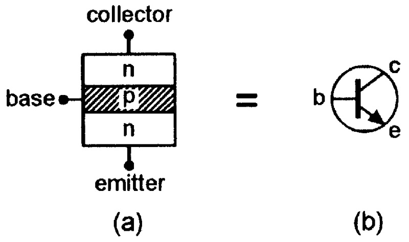
A normal transistor is made from a three-layer sandwich of n-type and p-type semiconductor material, with the base or “control” terminal connected to the central layer, and the collector and emitter terminals connected to the outer layers. If it uses an n-p-n construction sandwich, as in Figure 1(a), it is known as an npn transistor and uses the standard symbol in Figure 1(b).

 FIGURE 1. Basic construction (a) and symbol (b) of npn transistor.

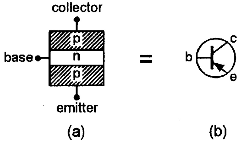
If it uses a p-n-p structure, as in Figure 2(a), it is known as a pnp transistor and uses the symbol in Figure 2(b).

FIGURE 2. Basic construction (a) and symbol (b) of pnp transistor.

In use, npn and pnp transistors each

Share:

Monday, 10 August 2020

7-segment LED Display


 An LED or Light Emitting Diode, is a solid state optical PN-junction diode which emits light energy in the form of “photons” when it is forward biased by a voltage allowing current to flow across its junction, and in Electronics we call this process electroluminescence.

The actual colour of the visible light emitted by an LED, ranging from blue to red to orange, is decided by the spectral wavelength of the emitted light which itself is dependent upon the mixture of the various impurities added to the semiconductor materials used to produce it.


Light Emitting Diodes have many advantages over traditional bulbs and lamps, with the main ones being their small size, long life, various colours, cheapness and are readily available, as well as being easy to interface with various other electronic components and digital circuits.

But the main advantage of light emitting diodes is that because of their small die size, several of them can be connected together within one small and compact package producing what is generally called a 7-segment Display.

The 7-segment display, also written as “seven segment display”, consists of seven LEDs (hence its name) arranged in a rectangular fashion as shown. Each of the seven LEDs is called a segment because when illuminated the segment forms part of a numerical digit (both Decimal and Hex) to be displayed. An additional 8th LED is sometimes used within the same package thus allowing the indication of a decimal point, (DP) when two or more 7-segment displays are connected together to display numbers greater than ten.

Each one of the seven LEDs in the display is given a positional segment with one of its connection pins being brought straight out of the rectangular plastic package. These individually LED pins are labelled from a through to g representing each individual LED. The other LED pins are connected together and wired to form a common pin.

So by forward biasing the appropriate pins of the LED segments in a particular order, some segments will be light and others will be dark allowing the desired character pattern of the number to be generated on the display. This then allows us to display each of the ten decimal digits 0 through to 9 on the same 7-segment display.

The displays common pin is generally used to identify which type of 7-segment display it is. As each LED has two connecting pins, one called the “Anode” and the other called the “Cathode”, there are therefore two types of LED 7-segment display called: Common Cathode (CC) and Common Anode (CA).

The difference between the two displays, as their name suggests, is that the common cathode has all the cathodes of the 7-segments connected directly together and the common anode has all the anodes of the 7-segments connected together and is illuminated as follows.

1. The Common Cathode (CC) – In the common cathode display, all the cathode connections of the LED segments are joined together to logic “0” or ground. The individual segments are illuminated by application of a “HIGH”, or logic “1” signal via a current limiting resistor to forward bias the individual Anode terminals (a-g).


Common Cathode 7-segment Display


2. The Common Anode (CA) – In the common anode display, all the anode connections of the LED segments are joined together to logic “1”. The individual segments are illuminated by applying a ground, logic “0” or “LOW” signal via a suitable current limiting resistor to the Cathode of the particular segment (a-g).


Common Anode 7-segment Display


In general, common anode displays are more popular as

Share:

Saturday, 8 August 2020

How to test RCDs ?

On Facabook:


Share:

Translate

Blog Archive

About Tesla Institute

My photo
Mission of TESLA INSTITUTE is to be the leading provider of scientific information on education in Electrical Engineering, Electronics, Automation and Computer Technology. TESLA INSTITUTE offer new teaching method. Generally our idea can be simple describe as: Problem -> Thinking -> Searching solution -> Real problem solution Big part of study at TESLA INSTITUTE school is realized as solving problems and practical real life projects, which give student many experiences already at school. So as alumni students of TESLA INSTITUTE have so many practical experiences for their future employers. Our alumni are ready to talk about real professional things on their job interview We teach, we share and spread knowledge. You are welcome to learn at TESLA INSTITUTE

Pages